Chip Centre - CDAC Bengaluru
With a fervent vision to make India a high-end Very Large Scale Integration (VLSI) design destination, Ministry of Electronics & Information Technology (MeiTY) has initiated Special Manpower Development Programme for Chips to System programme. This programme brings in a culture of System on Chip / System designing by developing working prototypes with societal applications. It enables the academic institutions to develop specialized manpower in the area of VLSI/ microelectronics and Chip to System development and broadens the base of ASIC / IC designing in the country.
A dedicated 'Chip Centre' has been established at C-DAC, Bengaluru to facilitate integration and fabrication of ASICs / Integrated Circuits designed under the SMDP-C2S program. Chip centre will act as a bridge between the designers and semiconductor foundries (SCL) in fabricating the IC. The objective of the Chip Centre is to enable fabrication of chips developed by Resource Centres and Participating institutes by means of Multi Project Wafer (MPW) services provided by Semi-Conductor Laboratory (SCL), Chandigarh.
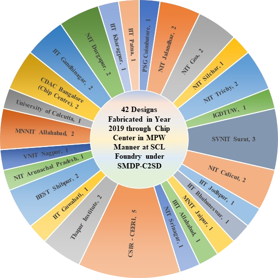
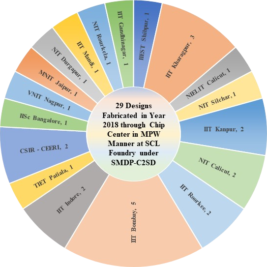
The Chip Centre receives tape-out ready designs from resource centres and participating institutions. The received designs are integrated. After integration of the designs, the integrated designs would be sent for fabrication to SCL, Chandigarh for Multi Project Wafer fabrication. A repository of proven designs/IPs will be setup and would be readily available for future use under the project.
The centre will interact with EDA vendors for setting up suitable EDA tools for ASIC design flow, full custom and semi-custom IC design flow, SoC design flow, Analog / Mixed-Signal flow at Chip Centre, and utilize the tools in integration of various ICs designed by institutions as part of SMDP-C2SD programme of MeitY. Call for chip tape out proposals will be made to solicit proposals from the institutions participating in the program as well as call to invite proposals from academic institutions other than RCs and PIs who can get their designs fabricated under the chip program will also be carried out. The Centre will also interact with the CIs of the participating institutions to work out the optimum utilization of silicon; providing IPs available in the repository for their future works. Further, the project includes design and development of IPs / SoCs by Chip Centre for specific end applications / domains.
The Chip centre is proposed to engage in the following activities:
- Facilitate Integrated Circuit tape outs and fabrication for institutions participating in the program.
- Interactions with SCL for MPW related fabrication schemes, technical requirements, hands-on-training on the foundry process design kits and establishment of common foundry libraries for all institutions under this programme.
- Interaction with EDA vendors and establishing the requisite EDA tools for Full-custom IC design flow, Semi-custom or cell based IC design flow, Analog / Mixed-Signal designs, SoC designs, etc. at Chip Centre.
- Integrating the tape-out ready designs received from various institutions as a multi-project chip targeting identified foundry (SCL or any other foundry) process needs and interacting with the foundries for fabrication.
- Fabrication of multi-project chips / dedicated chips (as needed) through multi-project wafer (MPW) flow of foundry (SCL or any other foundry) and providing the ICs to institutions.
- Interaction with SCL for chip tape out related activities and enable institutes to get the fabricated ICs.
- Design and development of IPs / SoCs by chip centre for specific end applications.
- Call for chip tape out proposals from other than SMDP-C2SD institutions for ASIC fabrication.
- Fabrication of multi-project chips / dedicated chips through multi-project wafer (MPW) flow of the foundry (SCL /other foundry) and providing the ICs to other than SMDP-C2SD institutions.
- Establishing a repository of validated designs and IP cores developed as part of SMDP-C2SD for design reuse as needed by the institutions.
- Organizing training on EDA tools for the institutions as per the requirement and thereby giving exposure to them on the chip design cycle from specification to chip fabrication. Such training will enable the academic students / researchers to enhance the competency level and prepare themselves better for the industry / academics. Such trained students will help the academic / research institutions to build prototypes of SoCs.
- Facilitating / enabling fabrication of designs and packaging of bare dies sent by foundry (SCL). Coordinating with the packaging firm in identifying the optimum package, arriving bonding diagram, obtain the packaged IC and provide to the institutions.
- Facilitating / enabling the institutions in testing of fabricated chips.
Contact Details:
C-DAC Knowledge Park,
Byappanahalli, Bengaluru - 560038.
+91-80-25093432
chipcentre[at]cdac[dot]in
C-DAC Knowledge Park,
Byappanahalli, Bengaluru - 560038.
+91-80-25093430
david[at]cdac[dot]in
C-DAC Knowledge Park,
Byappanahalli, Bengaluru - 560038.
+91-80-25093425
viviand[at]cdac[dot]in